Click the arrow down to see details about this chip.
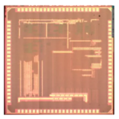
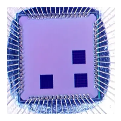
This was the first BIU analog tapeout. It included thermal sensors, as well as PUF circuits. The circuits exhibited excellent functionality and have generated publications in JSSC, TCAS1, SSCL, and ESSCIRC.
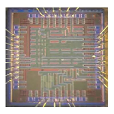
This follow-up tapeout included several new PUF circuits, all of which functioned well in Silicon. Papers were published in CICC and ISCAS 2019. Journal versions of these papers are being prepared at the present time.
This tapeout included PUFs, a Process Monitor and an ultra-low power bandgap reference. The circuits are fully functional and papers are being written.
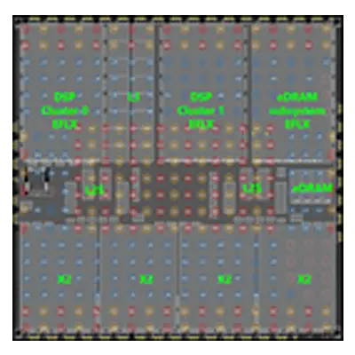
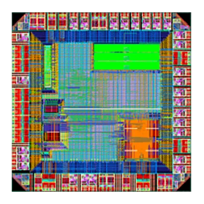
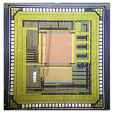
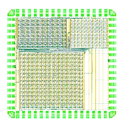
The second flagship demonstrator of the HiPer Consortium, this 11mm^2 system-on-chip was the first 16nm FinFET chip taped out by EnICS and was quoted by Cadence to be one of the most complex chips ever to be designed by an academic group. The SoC includes four CEVA-X2 cores, a Sonics NoC and three Flexlogic eFPGA, along with other peripherals. The primary innovation in the chip lies in the research demonstrators, including 1Mbit of Gain-Cell embedded DRAM, a Dual-Mode Logic based ALU, and an ultra-small, ultra-fast thermal sensor.
Circuits included a Ring-Oscillator based sensor, a mobility monitor and a Low Voltage Power-On-Reset Circuit. All circuits are functioning well and papers are being prepared.
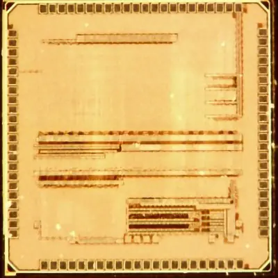
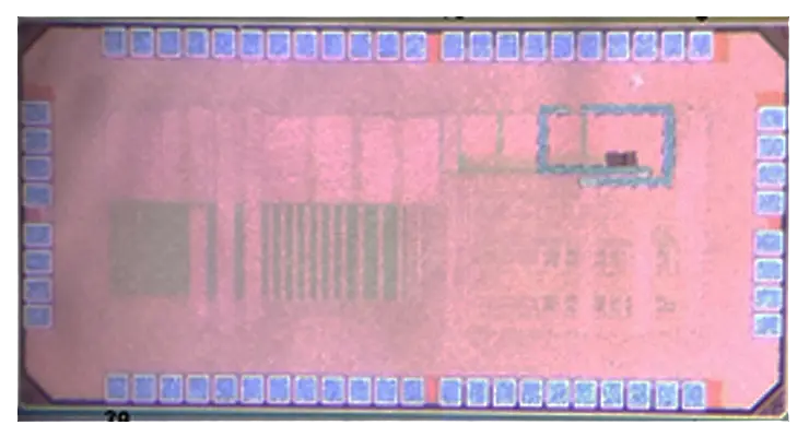
This chip contains an LDO, a Process Monitor, a Noise modeling circuit, two different Droop detector circuits, a Dual Mode Logic block, and a Switch-capacitor DC-DC converter.
This 28nm FD-SOI chip, designed in close collaboration with the TCL group at EPFL, includes two first of their kind Gain-Cell embedded DRAM blocks and a multiply-accumulate (MAC) unit, built with dual-mode logic (DML) gates. The results have been published in journals, such as TVLSI and TCAS-I.
* The acronym stands for “Bar-Ilan EPFL Embedded DRAM and Ramiro”
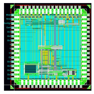
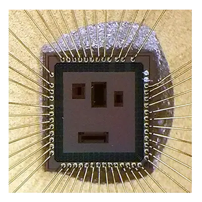
stands for Cryptography And Memory EnICS Labs (CAMEL) CHIP. This 65nm chip inhabits testing constructs for more than eight technologies to protect cryptographic implementations against physical Side-Channel-Analysis (SCA) attacks. Namely, protection of digital processing logic and low-lever register-based memories, several of our patents and many papers originated from this test-chip. Quite innovative and advances design techniques were used in the construction of this chip to allow low-noise measurements and security evaluation, including unique power-gated micro-pads access measurement points and advanced utilization of CPF flows. For details contact Dr. Itamar Levi.
stands for Trustworthy Reconfigurable Programmable Logic Array. In principle, originating from the hardware-security group, this unique ASIC incorporats a self-designed 65nm Secured-FPGA against SCA attacks. Specifically, several low-cost breakthrough signal-reduction and noise-insertion technologies are used for protecting the CLBs tailored for this structure. In the CHIP we have three different arrays of ~30×30 CLBs which is fairly large for an academic group test-chip, exhibiting excellent security with minor electronic properties cost. Moreover, we have developed unique automated tools to test, debug, program (i.e. load bitstreams) from functional specifications for the TRPLA. For details contact Dr. Itamar Levi.
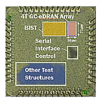
This 28nm bulk CMOS chip was designed and implemented in close collaboration with Mellanox as part of the HiPer Consortium. The chip was a demonstrator for the innovative 4T Gain-cell embedded DRAM bitcell, invented at EnICS. The results were presented at ESSCIRC and published in a special issue of JSSC.
Lorem Ipsum is simply dummy text of the printing and typesetting industry. Lorem Ipsum has been essentially unchanged.
Lorem Ipsum is simply dummy text of the printing and typesetting industry. Lorem Ipsum has been essentially unchanged.
This UMC 180nm test chip was fabricated in collaboration with the TCL group at EPFL. It included several GC-eDRAM arrays – one with improved replica for tracking retention time, one with test structures for device modeling and one with at 3T TG cell. It also included a 13T radiation hardened SRAM cell for subthreshold operation. The results were published in several ISCAS papers, TCAS-I, TVLSI and TCAS-II. This chip was also sent to undergo radiation testing in Belgium in collaboration with Soreq.
Lorem Ipsum is simply dummy text of the printing and typesetting industry. Lorem Ipsum has been essentially unchanged.
Lorem Ipsum is simply dummy text of the printing and typesetting industry. Lorem Ipsum has been essentially unchanged.
This 28nm FD-SOI was fabricated by the TCL group at EPFL with some EnICS blocks inside. The chip included a novel cycle-by-cycle dynamic frequency Open RISC core with results published at ESSCIRC and ISCAS. In addition, a 4T GC-eDRAM array was included and published in TCAS-I.
Lorem Ipsum is simply dummy text of the printing and typesetting industry. Lorem Ipsum has been essentially unchanged.
EnICS Labs | Bar-Ilan University
The Alexander Kofkin Faculty of Engineering
Building 1102 | floor -1, room 62
Ramat Gan 5290002
Israel